 |
|
|
Research
Topics |
|
■Objective
Research targets of the MBE electronics group
are establishment of formation technology of III-V semiconductor-based
quantum nanostructures, characterization and control of their surfaces
and interface, and their device application, utilizing advanced semiconductor
nanotechnology based on molecular beam epitaxy (MBE) crystal growth technology
and an unique UHV(ultra-high vacuum)-based process. These technologies
are applied to realization of ultra-high speed communication devices
and systems and ultra-high speed and ultra-low power consumption quantum
LSIs in order to realize ultra-small knowledge vehicles, IQ (intelligent
quantum) chips for future ubiquitous society.
■Research topics
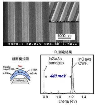
(1) Quantum nanostructure formation technology
Formation technologies of quantum dots (QDs)-
and quantum wire (QWR)-integrated structures by a selective MBE growth
technique are studied using GaAs-, InP- and GaN-based materials. Further
size reduction and high-density integration of the QDs and QWRs are intensively
studied, for realizing ultra-high density and large-scale integration
of quantum nanodevices and their high temperature operation. Ultra-high
density InP-based hexagonal nanowire networks with 109 nodes/cm2 have
been developed.
|
 |
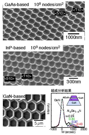 |
Fig.1 Quantum wire arrays formed by selective MBE
growth
|
Fig.2 Hexagonal quantum nanowire network structures
formed by selective MBE growth
|
|
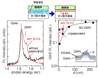
(2) III-V material's nano-surface/interface physics and nano-process
technology
In nanostructures and nanodevices, their surfaces
and interfaces come to play important roles in their properties and performances
remarkably. Nano-scale understanding of the surfaces and interfaces has
been made and original surface passivation technologies has been developed.
Such technologies has been applied to various devices, giving their high
reliabilities and performances. Especially, GaN-based materials have been
intensively investigated. Mechanism of anomalous leakage current in GaN
Schottky interfaces has been clarified in detail firstly and GaN-based
HFETs with completely stable operations have been successfully fabricated.
|
 |
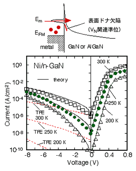 |
Fig.3 Surface passivation of selective grown (SG)
quantum nanowires
|
Fig.4 Analysis of leakage current in GaN Schottky
interfaces by Thin Surface Barrier Model
|
 |
|
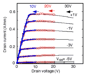
Fig.5 I-V characteristics
of Al2O3 insulated gate AlGaN/GaN HEMT
|
|
|
(3) Quantum nanodevices and novel integrated circuit technology
Unique quantum nanodevice technologies have
been established and improvement of their performances has been investigated.
Recently, a novel hexagonal BDD quantum circuit approach utilizing binary-decision
diagram (BDD) architecture and quantum nanowire networks was proposed,
which has high capability for realization of quantum LSIs in a realistic
way. Based on this approach, ultra-small and ultra-low power consumption
digital systems, such as nanoprocessors, which further exceed previous
Si LSIs and systems, have been studied for IQ chips.
|
 |
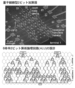 |
Fig.6 I-V characteristics of quantum wire transistors
and single electron transistors.
|
Fig. 7 (a)Fabricated hexagonal BDD 2-bit adder
and (b) ALU design.
|
|
(4) Ultra-high frequency devices and sensing devices
As key devices in the future ubiquitous society,
ultra-high frequency devices for wireless communications and sensing devices
have been studied. The aim of this study is to realize such devices having
ultra-small size, ultra-high efficiency, ultra-high speed and ultra-high
sensitivity, by combination of III-V compound semiconductors with high
speed carrier transport, nanostructures and quantum physics. Novel communication
and sensing devices have been developed as shown in Figs.4 and 5 for IQ
chips.
|
 |
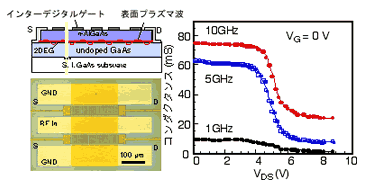 |
Fig.8 On-chip antenna and rectenna
|
Fig. 9 Electric-Magnetic wave-semiconductor surface
plasma wave interaction device
|
 |
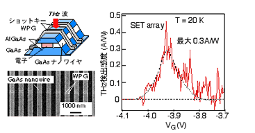 |
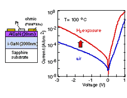
Fig.10 AlGaN/GaN-based Hydrogen gas sensor using
Pt Schottky gate.
|
Fig.11 THz wave detection using quantum wire array
|
|
|
